
Abstract
Recently, logic gates comprised of DNA reaction systems have been investigated in the field of DNA computing. An XOR gate, a type of logic gate, can be applied in certain applications, such as encryption and as a half subtractor. In theory, the XOR gate can be fulfilled by combining basic operators (AND, OR, and NOT gates). However, the XOR gate involves 83 DNA strands because it requires two AND gates, an OR gate, and two NOT gates. The XOR gate is a complicated reaction system and is almost impossible to achieve. Accordingly, we optimized the XOR gate and decreased the number of DNA strands from 83 to 22. This resulting reaction system operated faster than the XOR gate comprised of the basic operators. We obtained an optimized XOR gate, using this novel “trick”; therefore, we called this gate “Trick XOR Treat.”Our Project
1. Background
We focused on the possibility of molecular computing of calculation capability. We attempted to realize the four arithmetic operations with the logic gates (AND, OR, NOT, XOR, NAND, and NOR gates). Since we incorporated these gates into a DNA circuit, we required a reaction system with reliable, quick operation capacity. Basic operators (AND, OR, and NOT gates) have already been realized in DNA reaction systems; thus, the XOR gate could be realized, in theory, by combining these operators. However, the combinational circuit is highly complex because an XOR gate requires two AND gates, an OR gate, and two NOT gates. Accordingly, in this study, we focused on the XOR gate as an operator for molecular programming and aimed to design an XOR gate having a simple reacting system without the basic operators.

Figure 1 : The difference of the Trick XOR Treat with the combinational XOR circuit
2. What is logic gate
A logic gate is a circuit that carries out a logic operation. In general, a logic gate has two inputs, which are divided into high and low according to a threshold.
A logic circuit is the smallest modules making up a digital circuit and is therefore essential for electrical products. Similarly, when we produce some systems, we need the smallest modules; accordingly, it is necessary to use the smallest modules when we produce something in DNA reaction systems. Therefore, we need a logic gate when we produce systems using DNA.
ANDgates, ORgates, and NOTgates can be used in logic gates[1,2]. Their functions are expressed by a truth table. ANDgates, ORgates, and NOTgates are called basic logic gates. In general, we can make one-step large modules, i.e., XORgates, NORgates, and NANDgates, by combining basic logic gates. Moreover, we can make larger modules, e.g., flip-flops, and registers by combining XOR, NOR, NAND, and basic logical gates. We can make a product such as a microcomputer by repeating combining modules. Because computers are machines for computing, as the name suggests, modules for computing are required. One such module is called an accumulator, which requires XOR. Like this, XOR is used in various ways. Thus, XOR is an important module which is worthy to be made.
3. Project Idea
The XOR gate functions as shown in the truth table in Table 1. The XOR gate used in our analysis considers the concentration of DNA as the input in a DNA reaction system. The output of the system is “high” when only “high” or “low” is input as the concentrations; otherwise, when “high-high” or “low-low” are input as the concentrations, the output is “low”.

As described in section 2, a large module is made by combining small modules. First, we considered creating XOR by combining AND, OR, and NOT; however, many DNA strands are required, and the reaction system becomes quite complex. Complex reaction systems are difficult to use, particularly for DNA reaction systems, because complex conditions tend to favor reactions that are not the target reaction. Moreover, more complex reaction systems exhibit slower reaction velocities. To overcome these problems, we designed the “Trick XOR Treat” system, as explained on the Design page. The XOR gate presented in this report was designated “Trick XOR Treat.” Trick XOR Treat overcame the shortcomings of XOR, using a combinational circuit. XOR combined with AND, OR, and NOT requires many DNA strands (i.e., 83 strands); however, our Trick XOR Treat system alone could perform the functions of XOR, using a few strands (i.e., 22 strands). Moreover, the Trick XOR Treat was faster than combinational XOR with regard to the reaction velocity. The difference in the reaction velocity is 150 min.
4.Goals reached
Our first goal was realizing XOR in a DNA reaction system.
1. We designed Trick XOR Treat, a new XOR gate functioning in a DNA reaction system.
2. We simulated Trick XOR Treat and the combinational XOR circuit.
3. We verified Trick XOR Treat through experiments.
Our second goal was investigating the applications of XOR.
4. We designed the half subtractor as the application of XOR.
5. We simulated the half subtractor.
6. We performed experiments for generation of the subtractor.
We have achieved all goals to generation of the application of XOR.

Figure 2 : Project goal and achievement
Design
Reaction path of Trick XOR Treat
We designed the Trick XOR Treat system based on strand displacement reactions. This gate was composed of four DNA strand displacement reaction processes. Each of these reaction processes is explained below.
First Process:
In first process, we aimed to make the models Next1-1 and Stop1, using a strand displacement reaction.
1. T1 of Makestopper1 is bound with T1* of Input1.
2. Makestopper1 and Input1 are effectively combined.
3. A part of Makestopper1 separates from the complex.
4. Next1-1, Stop1, and Waste are generation by separating the components.

Figure 3 : Schematic diagram of the first process 1. ※Click for larger image

Figure 4 : Schematic diagram of the first process 2. ※Click for larger image
Second Process:
In the second process, we aimed to generate a model of Next1-3 and Next2-3 through a strand displacement reaction, similar to the first process. This process utilized Next 1-1 and Next2-1, which were produced in the first process.

Figure 5 : Schematic diagram of the second process 1. ※Click for larger image
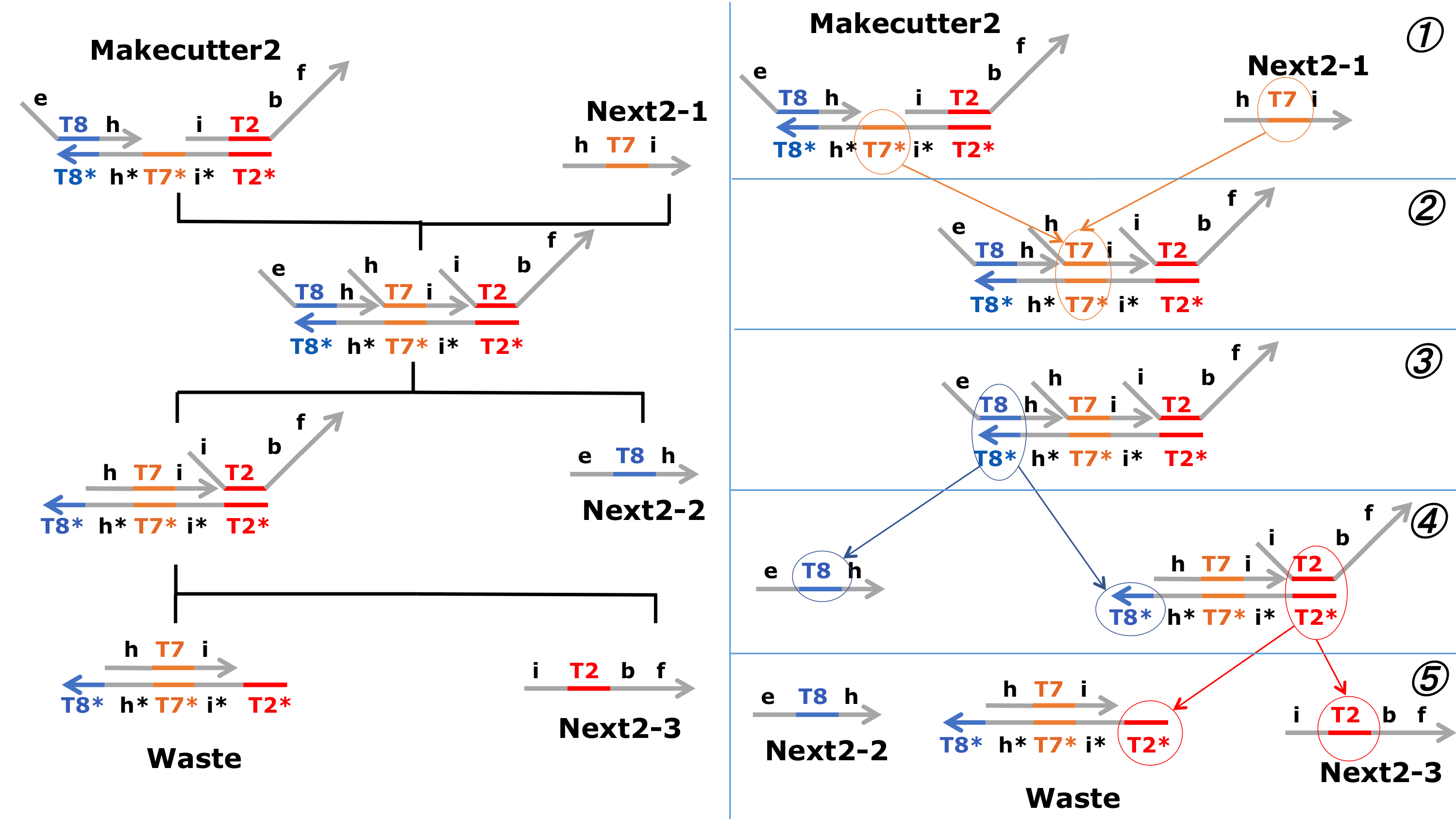
Figure 6 : Schematic diagram of the second process 2. ※Click for larger image
Third Process:
In the third process, there are two types of reactions.
First, we aimed to generate Next1-4, using a strand displacement reaction.
1. T4* of Makeoutput1 is bound with T4 of Next1-2.
2. Makeoutput1 and Next1-2 are effectively combined.
3. T5 of Next1-3 is bound with T5* Makeoutput1, and the part generated in the previous step separates.
4. Next1-4 and two types of Wastes are generated by dividing and combining these components.
Next2-4 is produced according to a similar method.

Figure 7 : Schematic diagram of the third process 1. ※Click for larger image

Figure 8 : Schematic diagram of the third process 2. ※Click for larger image
First, we aimed to generate Next1-5, using a strand displacement reaction.
1.aT5* of Makeoutput1 is not bound with T5 of Next1-3, and aT5* of Makeoutput1 try to be bound with aT5 of Stop2.
2.Makeoutput1 and Stop2 became to combine, b of Makeoutput1 is separated from Makeoutput1 because of combining.
3. T4 of the production in the before step try to combine with T4 of Next1-2.
4. Next1-5 is produced by that combining, and b separated from Makeoutput1 is Waste.
Next2-5 is produced according to a similar method.
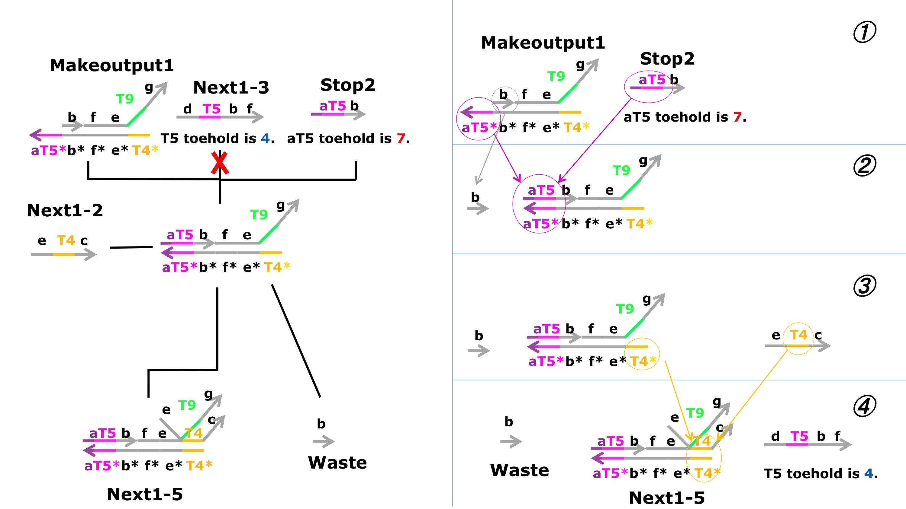
Figure 9 : Schematic diagram of the third process 3. ※Click for larger image

Figure 10 : Schematic diagram of the third process 4. ※Click for larger image
Fourth Process:
This is the final process. T9* of the Reporter1 is bound with T9 of Next1-4 or Next2-4. At this time, the product is Waste, and domain "e f" is the part of Reporter1 that separates because of the complex formation. This is the Reporter1 output.

Figure 11 : Schematic diagram of the fourth process. ※Click for larger image
Material & Methods
1.Simulation Condition
We set the rate constant based on toehold length as follows [4,5].

2.Type of strands
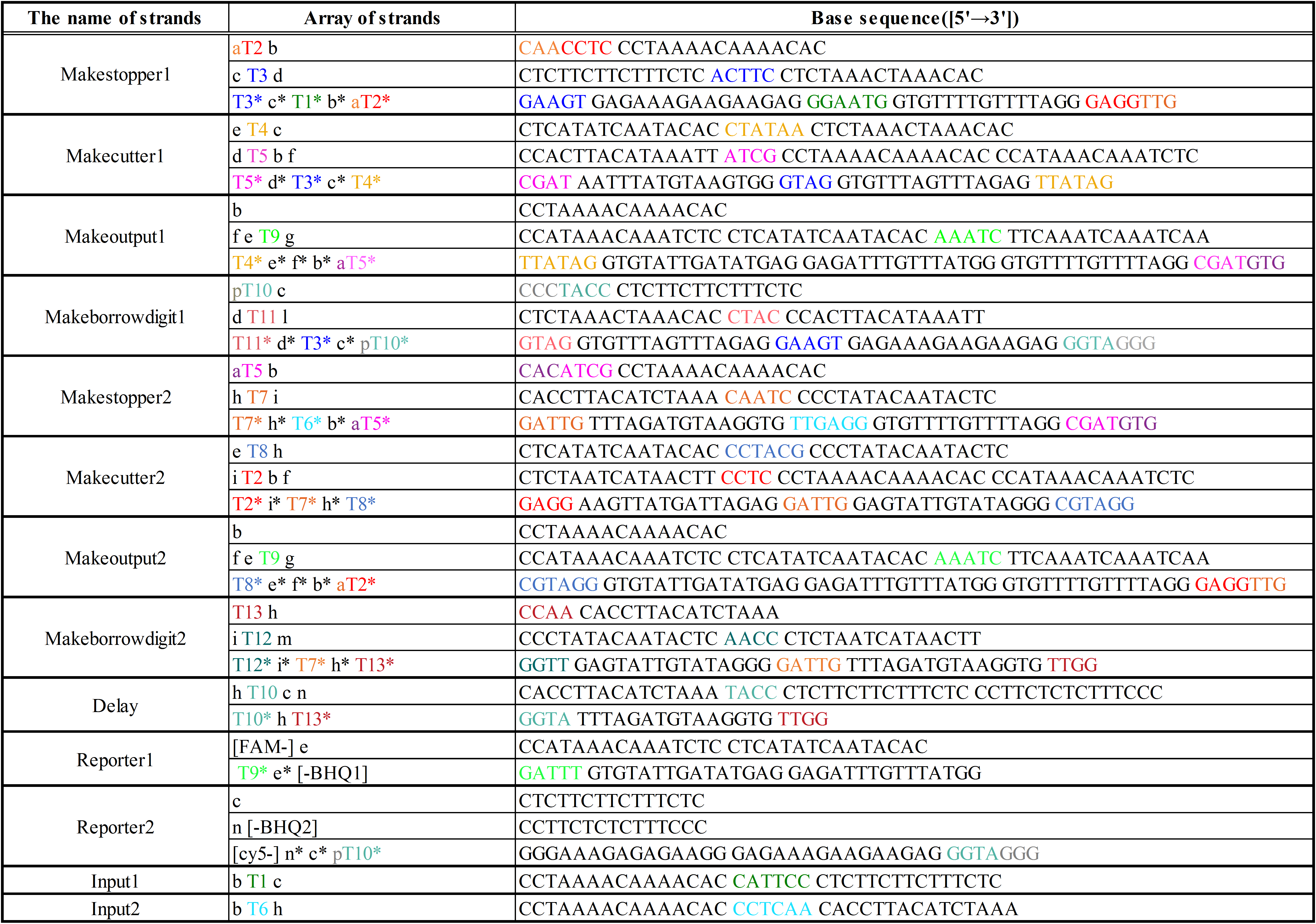
We designed the strands shown in Figures 12~17.
 |
 |
 |
 |
 |
 |

In addition to these strands, we prepared the strand shown in Figure 18 to confirm whether the output was released.
Additionally, we designed DNA sequences by visual DSD[5] and NUPACK[6]. The DNA sequences are shown below in Table 2. Visual DSD is a software which simulates and analyzes DNA strand displacement reactions, and can be utilized as a programing language for a computer-aided design of DNA circuits. On the other hand, NUPACK can design the DNA sequences, and evaluate their secondary structures at a room temperature.

The colored portions show the toeholds, with the colors corresponding to those shown in Figures12~18.
In addition, input DNAs and their DNA sequences are shown in Figure 19, Figure 20, and Table 3.
The colored portion shows the toehold, with colors corresponding to those in Figures 19 and 20.


We then performed experiments using these strands, as described below.
3.Wet Experiment of Trick XOR Treat

Step.1 Dilute
We diluted each strand until reaching the desired concentration, as shown in Table 4 below. The experiment was performed at 20°C in Tris-EDTA buffer supplemented with 12.5 mM MgCl2.
We conducted four types of experiments:

Each initial input concentration is shown in Tables 5~8 above. We set the input concentration to 200 nM when the input was “High” and to 0 nM when the input was “Low”.
Step.2 Annealing
We annealed each DNA in Table 4 from 95 to 20°C (-1°C/min) after heating at 95°C for 15 min.

Figure 21 : Thermal cycler (ASTEC325; GeneAtlas) [used for annealing]
Step.3 Reporter intensity measurements
We measured the Reporter intensity using a spectrofluoremeter (FP-8300; JASCO) for 5 h with 5-min intervals.

Figure 22 : Spectrofluoremeter (FP-8300; JASCO)
4.Output confirmation
We applied FRET to confirm how much output was released. Before the output reacted with Reporter, the FAM did not fluoresce since the Reporter of FAM was absorbed by BHQ1. When output reacted with Reporter, the Reporter of FAM became detectable because the distance between the FAM and BHQ1 molecules increased (Figure 23).

Figure 23 : Output confirmation
Experiment
Dry Experiment
We simulated the output concentration of the Trick XOR Treat using numerical software (Matlab[7]); the performance and refinement are described herein. The threshold concentration was defined as 50 nM,
where “High” > 50 nM and “Low” < 50nM. We conducted four types of simulations: Pattern1, Input1 and Input2 were “Low”; Pattern2, Input1 was “High” and Input2 was “Low”; Pattern3, Input1 was “Low” and Input2 was “High”; and Pattern4, Input1 and Input2 were “High”. In addition, we set the initial input concentration at 200 nM (High) or
0 nM (Low).
1.Confirmation of the output concentration for the Trick XOR Treat
When Input1 and Input2 were added to the Trick XOR Treat, we simulated the output concentration. Figure 25 shows the four simulation patterns.

Figure 24 : Trick XOR Treat schematic


|

|

|

|
2. Comparison of the Trick XOR Treat with the combinational XOR circuit
As shown in Figure 26, the XOR circuit can be designed to combine the ANDgate, ORgate, and NOTgate.

Figure 26 : Combinational XOR circuit schematic
Realization of the combinational XORgate is difficult because the complex circuits in the DNA reaction system tend to cause unwanted reactions. We compare simulations between the Trick XOR Treat and combinational XOR to determine which exhibited a simpler design.

Table 9 shows that the design using the Trick XOR Treat was simpler because each number was lower. Thus, we then compared simulations using both approaches.

Figure 27 : Simulations

Figure 28 : Expansion of Figure 27 , with the time scale changed to minutes
The graphs above show High-Low outputs because the concentration for the Low-Low output was less than 10^(-8) M.
We found that the output was “Low” when the graph’s value was comparatively low. Therefore, we set the threshold as 50 nM. With this threshold, the design using the Trick XOR Treat was faster than the other design when the output was “High”. Because the threshold concentration was 50 nM, as shown in Figure 28, the output became “High” at 150 min. If we used the combinational circuit, 150 min may be a critical weak point. Our Trick XOR Treat overcame this limitation.
Wet Experiment results
As shown in the table below, we separated our experiment into pattern1, pattern2, pattern3, or pattern4, and conducted experiments of the Trick XOR Treat.
We make a complex of Input1, Input2, Makestopper1, Makestopper2, Makeoutput1, and Makeoutput2 and wait for 6000 seconds in pattern4. After that, we added Makecutter1, Makecutter2, and Reporter1 to the complex and measured the change of time of fluorescent strength. In this way, Stop reacted with Makeoutput certainly, and we show the graph normalized by fold-change.

1) Pattern1: Input1 = 0 nM(“Low”), Input2 = 0 nM(“Low”)

Figure 29 : Experimental results for Pattern1
2) Pattern 2: Input1 = 200 nM("High”), Input2 = 0 nM(“Low”)

Figure 30 : Experimental results for Pattern2
3) Pattern 3: Input1 = 0 nM(“Low”), Input2 = 200 nM(“High”)

Figure 31 : Experimental results for Pattern3
4) Pattern4: Input1 = 200 nM(“High”), Input2 = 200 nM(“High”)

Figure 32 : Experimental results for Pattern4

Figure 33 : Experimental results for Pattern1~4
It was found from this graph that we distinguished Low of output from High of output. Moreover, we obtained the result we surmised from the simulation.
Application
We devised the following four systems as application using Trick XOR Treat.
1.Half subtractor
1.1 What is half subtractor
The half subtractor is a subtracting circuit used for two input data. As shown in Table 11, the outputs were the Difference and the Borrow digit, the half subtractor operated normally using the Difference and the Borrow digit. Figure 34 shows an example of subtraction in the bit1. As shown left in figure 34, if we calculated 0 - 1, we needed to borrow value from bit2. When we borrowed value, Borrow digit equaled to 1(“High”). In this way, the calculation in bit2 was performed correctly.


Figure 34 : The substraction of binary number in two bits
1.2 Reaction
The Difference was the output of Trick XOR Treat, and the half subtractor reaction was based on the Trick XOR Treat reaction system. As shown Figure 35, by adding Makeborrowdigit, Delay, and Reporter2 in the initial state, we obtained outputs of Difference and Borrow digit.

Figure 35 : Reaction sequence of the half subtractor.
Each of these reaction processes is explained below.
First Process:
Input1 causes a strand displacement reaction with Makestopper1, yielding Next1-1. Similarly, Input2 reacted with Makestopper2, yielding Next2-1.
Second Process:
As shown Figure 36, Next1-1 reacted with Makeborrowdigit1, yielding Next1-6 and Stop3. Alternatively, Next2-1 reacted with Makeborrowdigit2, yielding Next2-6 and Next2-7. Next1-6 and Next2-6 were used to obtain the Difference, and Stop3 and Next2-7 were used to obtain the Borrow digit.

Figure 36 : Schematic diagram of the second process. ※Click for larger image
Third Process:
For the Difference reaction, Next1-6 reacted with Makecutter1, yielding Next1-2 and Next1-3. Alternatively, Next2-6 reacted with Makecutter2, yielding Next2-2 and Next2-3. We omitted the subsequent reactions because they were similar to the reactions described on the Design page.
The Borrow digit and Difference reactions occurred at the same time. As shown Figure 37, Next2-7 reacted with Delay, yielding Next2-8.
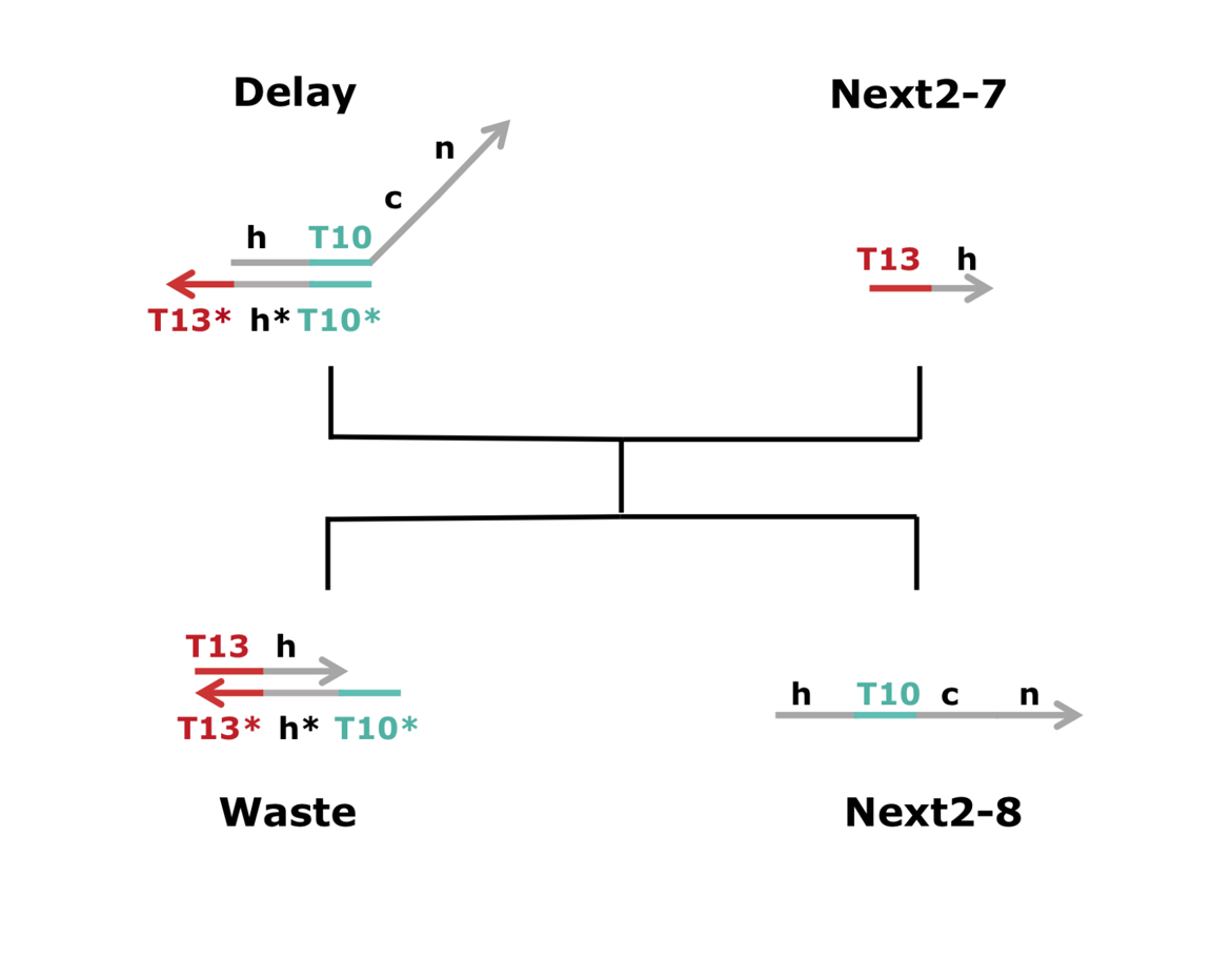
Figure 37 : Schematic diagram of the third process. ※Click for larger image
Fourth Process:
As shown Figure 38, Stop3 reacted with Reporter2, yielding Waste. As a result, the Borrow digit value was “Low” (0). In this case, the toehold length of Stop3 was 7 (nt), and the toehold length of Next2-8 was 4 (nt); therefore, the reaction rate of Stop3 was faster than that of Next2-8. In addition, the reaction time of Next2-8 was slower than that of Stop3 because of the Delay step shown in Figure 17. For this reason, Stop3 caused a strand displacement reaction with Reporter2 in the first process, and Next2-8 barely reacted with Reporter2. If the Input1 concentration was “Low,” Stop3 did not occur. Therefore, Next2-8 reacted with Reporter2, yielding Reporter2 output, as shown Figure 38, and the Borrow digit was “High” (1).

Figure 38 : Schematic diagram of the fourth process. ※Click for larger image
1.3 Simulation
We simulated the output concentration of the half subtractor, using numerical software (Matlab [1]). The threshold concentration was defined as 50 nM, where “High” was greater than 50 nM, and “Low” was less than 50 nM. We conducted four types of simulations: Pattern1, Input1 and Input2 were “Low;” Pattern2, Input1 was “High” and Input2 was “Low;” Pattern3, Input1 was “Low” and Input2 was “High;” and Pattern4, Input1 and Input2 were “High.” In addition, we set the initial input concentration at 200 nM (“High”) or 0 nM (“Low”) (Figure 39).

|

|

|

|
1.4 Material & Methods
We prepared the strands shown in Figure 40~43, and also prepared the new strands in Figure 40~43 in the experiment of the half subtractor. The DNA sequences are shown below in Table 12.
 Figure 40 : Makeborrowdigit1 |
 Figure 41 : Makeborrowdigit2 |
 Figure 42 : Delay |
 Figure 43 : Reporter2 |

1.5 Experiment
In the half subtractor, we conducted four kinds of experiment as the experiment of Trick XOR Treat.
1) Pattern1: Input1 = 0 nM(“Low”), Input2 = 0 nM(“Low”)

Figure 44 : Experimental results for Pattern1
2) Pattern 2: Input1 = 200 nM("High”), Input2 = 0 nM(“Low”)

Figure 45 : Experimental results for Pattern2
3) Pattern 3: Input1 = 0 nM(“Low”), Input2 = 200 nM(“High”)

Figure 46 : Experimental results for Pattern3
4) Pattern4: Input1 = 200 nM(“High”), Input2 = 200 nM(“High”)

Figure 47 : Experimental results for Pattern4
From Figure44 to Figure47 shows that the experiments result of Borrow digit matched the simulation. However, the output of Difference was lower than we had expected and the difference between High and Low was small in Pattern2 or 3. We had concluded that the systems which produced Differece may be affected. This was why the number of DNA strands which associated with this reaction was increased because of incorporating the systems producing Borrow digit.
2.Half adder
The half adder is the opposite application as the half subtractor and can add binary numbers of a single digit. Truth table is show in Table 14 below.

The half adder has two outputs, and Carry out becomes 1 only when the carry occurs. This application can be generated by combining the XOR and AND gates in the combination circuit. The circuit diagram is shown in Figure 48.

Figure 48 : The circuit diagram of the half adder
The basic circuit used in the half adder is only two; therefore, fewer DNA strands are required. Consequently, we believe that the half adder can be used in a combinational circuit in a DNA reaction system. However, we can generate a half adder without a combinational circuit if we use the method used to generate the half subtractor.
3.Encryption
Notably, XOR is a characteristic that is suitable for encryption and can be returned to the original, using the XOR gate with the same value twice. A specific example of this characteristic is shown in Figure 49 below.

Figure 49 : The properties of the XOR gate.
There are two data with 4 bits of information. We set these as inputs of the XOR circuit. Then, the Output will be as shown in the center of Figure 49 above. Next, we set this Output and Input2 as Inputs. Thus, the Output is the same as the first Input1. This is a characteristic of the XOR circuit. We can create an encryption such that the encryption key and decryption key are the same based on this characteristic. This encryption is called simple substitution cipher. Thus, we can use XOR as a key. When applied in a DNA reaction system, we can protect the information of the nucleotide sequence of DNA by encryption.
4. Introduction of the threshold gate
Through simulation with the Trick XOR Treat, when Input1 was “Low” and Input2 was “Low”, the output concentration was nearly equal to Input1 plus Input2. For this reason, connecting the Trick XOR Treat as shown in Figure 50, the output concentration gradually increased and would be “High”, despite that both inputs were “Low” (Figure 51). In order to overcome this problem, we attached a threshold gate to the Trick XOR Treat. Figure 53 shows the function of the threshold gate, which divided the input concentration into “High” or “Low” as a border threshold concentration. If the input concentration was “Low” after passing the threshold gate, the output concentration would be 0.5 nM. For this reason, the output of the Trick XOR Treat attached to the threshold gate would not ever “High”, when both Input1 and Input2 were “Low”.
 |
 |
 Figure 52 : XORgate with the threshold gate schematic |
 Figure 53 : Threshold gate function |


|

|

|

|
Member

Team Member
Undergraduate Students
B2 Yamamoto,Yuto
B4 Aosaki,Yuya
B4 Tanaka,Yuki
B4 Hidaka,Taisei
B4 Misawa,Michiko
B4 Yoshida,Yuki
Graduate Mentors
M1 Omagari,Tomotaka
M1 Nishijima, Katsuhiro
M1 Ogata, Kento
Faculty Mentor
Associate Professor Nakakuki,Takashi
Refference
[1] L. Qian and E. Winfree: Scaling Up Digital Circuit Computation with DNA Strand Displacement Cascades, Science, Vol. 332, No. 6034, pp.1196-1201, 2011.[2] L. Qian and E. Winfree: A Simple DNA Gate Motif for Synthesizing Large-Scale Circuits, J.R.Soc.Interface, Vol. 8, No. 62, pp. 1281-1297, 2011.
[3] D. Zhan and E. Winfree: Control of DNA Strand Displacement Kinetics using Toehold Exchange,J. Am. Chem. Soc, Vol. 131, pp. 17303-17314, 2009.
[4] S. Kobayashi, K. Yanagibashi, K. Fujimoto, K. Komiya and M. Hagiya:
Analog DNA Computing Devices Toward the Control of Molecular Robots, Workshop on Self-organization in Swarm of Robots: from Molecular Robots to Mobile Agents (WSSR 2014), Nara, Octorber, 2014.
[5]Programming DNA circuit (Visual DSD):
https://www.microsoft.com/en-us/research/project/programming-dna-circuits/
[6]Nupack:
http://www.nupack.org
[7]Matlab:
http://jp.mathworks.com/products/matlab/
[8] C. Thachuk, E. Winfree, and D. Soloveichik : Leakless DNA Strand Displacement Systems, DNA Computing and Molecular Programming, Vol.9211, pp 133-153, 2015.